Mattson Technology Atomic Surface Engineering™ and Atomic Interface Engineering™ equipment and services address some of the most critical logic and memory manufacturing challenges. Continuous integrated circuit device scaling includes fabrications of small, deep and complex 3D structures composed of thin layers of different materials. Manufacturing requires ultra-high selectivity in materials removal processes, and a precise control of physical, chemical and electrical properties of thin film surfaces.
For additional Atomic Surface Engineering™ and Atomic Interface Engineering™ product and servicing information for the equipment for the treatment and processing of semiconductor substrates and other semiconductor workpieces, see:
Novyka® Family Selective Etch Systems
Novyka® Family Surface Treatment Systems
Novyka® Family Surface Treatment and Interface Treatment Systems
For Atomic Surface Engineering™ and Atomic Interface Engineering™ sales information, contact our sales team at: info@mattson.com. For Atomic Surface Engineering™ and Atomic Interface Engineering™ servicing information for the servicing of equipment for the treatment and processing of substrates and other workpieces, contact our sales team at: info@mattson.com.
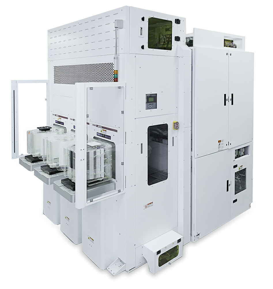 Novyka® Product Family
Based on an industry leading remote plasma technology, Mattson Technology’s Novyka® family selective etch systems offer unique process solutions and deliver outstanding results in isotropic and anisotropic etch of various dielectric and conductor materials.
As part of our Atomic Surface Engineering™product portfolio, the Novyka® family selective etch processes are ideal in efficient removal of thin and delicate layers in construction of advanced 3D transistor and capacitor structures.